Project information
- Category: Hardware
- Client: Personal
- Project date: Spring 2022
Project Objective
Learn reflow soldering to allow soldering of tiny components, and practice PCB design using Altium.
Overview
I really wanted to learn reflow soldering. It would be essential for the flight computer product due to the small size of the components. But I needed to develop a board to practice with, and also had to learn Altium anyway to help out on the Rocket Team. This brought the 555 Square Wave Oscillator project to life. I needed a circuit design that was impossible to solder completely by hand to force the need for reflow soldering for full functionality. The 555 oscillator is a circuit I am familiar with, but also more complex than the Counter from the previous PCB project so I would also get practice with PCB design software. There was also enough variety of components for me to test reflow soldering with. I also wanted to add a particularly particularly small component to test the limits of this method. This would ideally be a non-essential component so that the rest of the circuit is still functional if it does not get soldered correctly.
Final Product
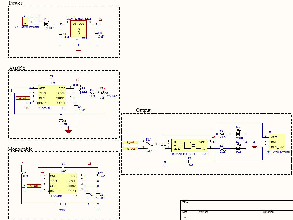
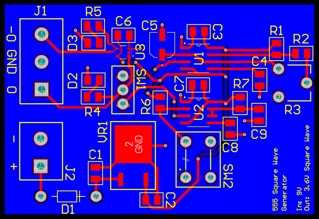
The final design takes in between a 6-18V (although higher voltage is not reccomended, as a cooling solution was not built in) supply which is then regulated down to 5V. There is a diode in place for reverse polarity protection. The board will output a 5V clock, as well as its inverse. The clock can either be from the 555 in astable configuration or in monostable configuration. This means that its possible to get an automatic clock, up to about 510 hz, or a manual clock from a debounced momentary switch. The astable clock frequency is adjustable using a 1MΩ logarithmic potentiometer. The bottom layer is also a ground plane, which is a large improvement over the previous PCB. Altogether the cost is about $10 USD per board, although parts were mostly bought individually rather than in bulk, making it a bit more expensive.
Conclusion
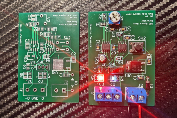
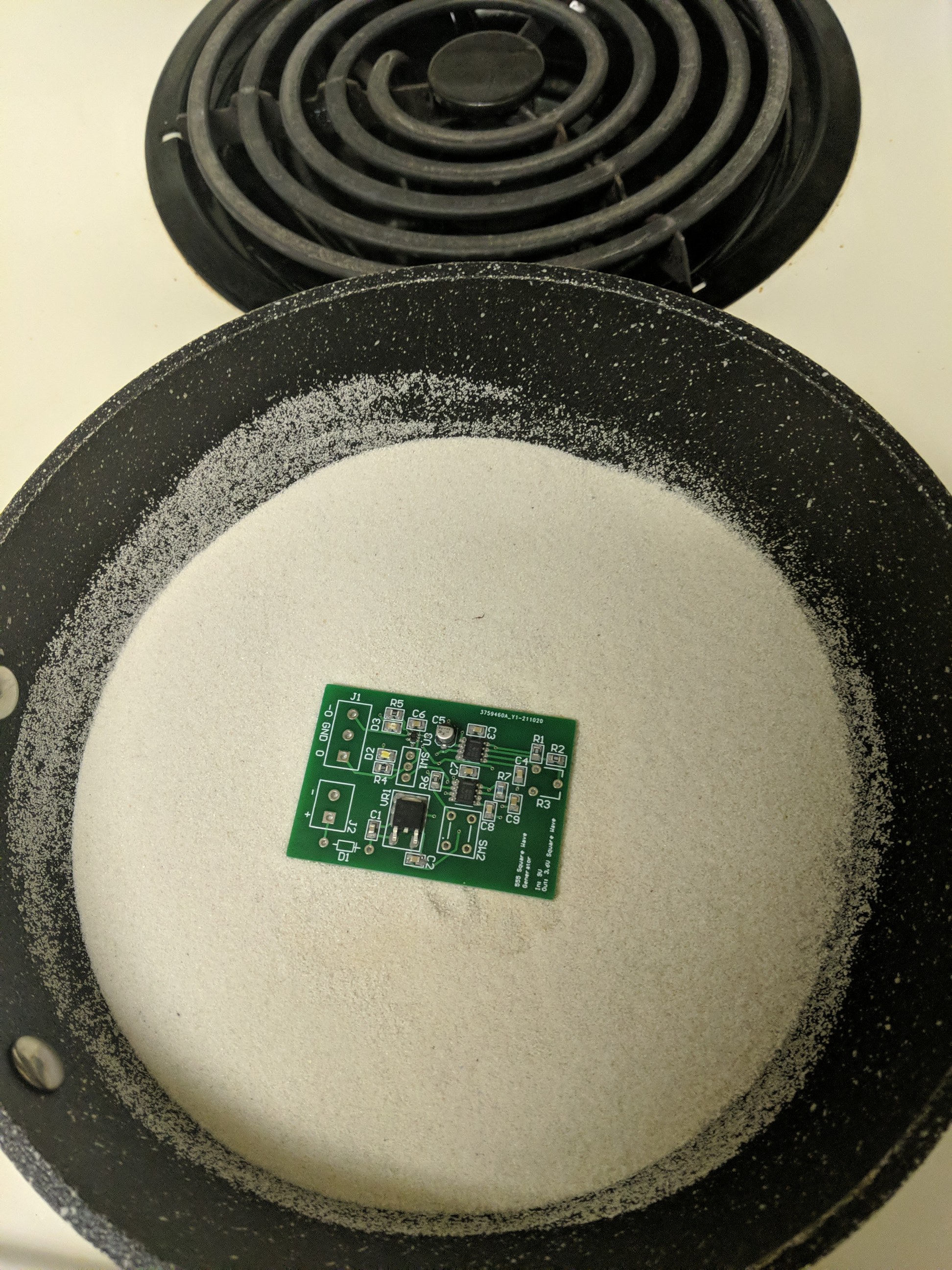
Reflow soldering turned out to be a huge success. Every single surface mount component was mounted on the board on the very first try, including both the voltage regulator, the largest component, and the NAND gate, the smallest component. Additionally, a reflow oven was not used (they cost upwards of $2000). Instead, the board was placed on a small layer of fine sand which was then heated by a stove until the solder past melted and became shiny. The sand spreads the heat out more evenly. However, I learned you have to be careful on the type of sand that you purchase. This sand seemed to have quite a few impurities and produced an irritating smoke (too much to be from the board itself). Thankfully, ovens conveniently come with vents which allowed me to get rid of this smoke pretty easily, but in the future I will need to do more research on a better brand of sand.
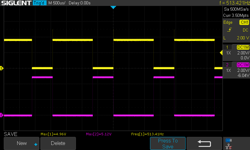
Onto the board itself, it exceeded expectations. During prototyping, the output clock was hovering around 3.6V, however this was deemed acceptable as it is enough to trigger a high clock pulse, and the focus of the project is Altium and the soldering anyway. But the final PCB outputs just about 5V (yellow wave on the figure below), and its inverse signal (the purple wave), outputs a little above 5V. This is likely due to it being the output from the NAND gate, an active component which can, in a way, boost the voltage back up to slightly above 5V. The maximum frequency can vary slightly between 510 - 515 hz, but otherwise is quite reliable. The minimum frequency is about .8 hz. An interesting note about this is that while the frequency is solid, the duty cycle of the signal has issues for a clock signal. The duty cycle is the amount of time the wave spends on versus the time it spends off. A 555 oscillator has the flaw where its duty cycle varies with frequency. This is due to 2 resistors. The main capacitor charges up through R1, R2, and R3, while discharing through only R2 and R3. I will treat R2 and R3 as the same resitor since R2 is meant only to avoid a short when R3 goes to zero. When the clock is slow, R2R3 is much larger than R1, this small ratio makes the charge and discharge time of the capacitor essentially the same. So at a slow clock the duty cycle is right around 50%. However as the clock speeds up, the ratio from R2R3 and R1 gets much close to 1. Making the worst difference in duty cycle. In my case it ends up being about 66% of the time on, 34% of the time off. Counterintuitively, its spends more time on, but an easy was to think about it is that its got a really fast discharge, so as soon as a discharge is triggered, it drops to 0V rapidly, it slowly charges back up and ends up spending a lot of time in that charging state, especially since capacitors charge slower as they gain charge. The one thing I would do differently on future PCB's would be to how a power plane on the top layer, instead of just a ground plane on the bottom layer.
